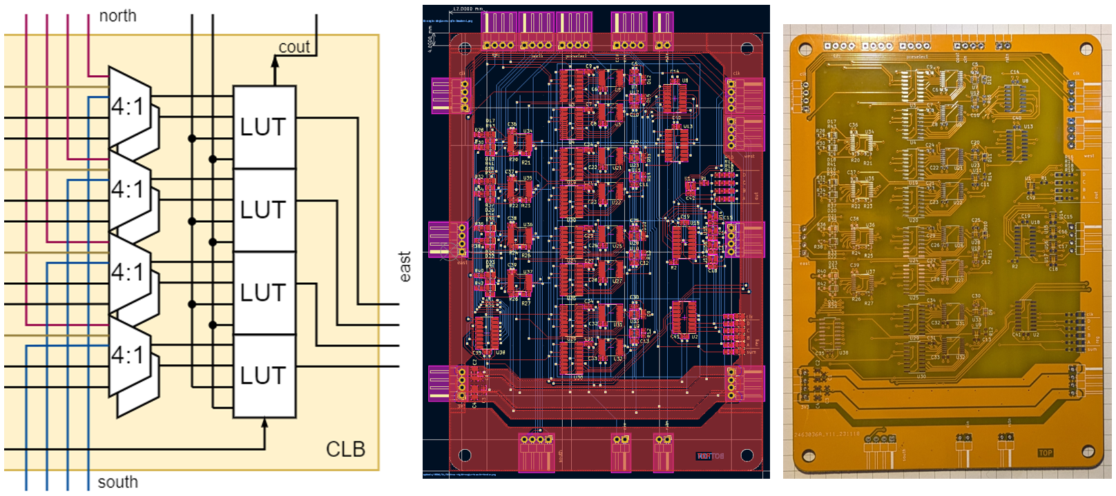
 Fig 1: The CLB from concept to PCB.
Today, my fellow FPGA nerd, I proudly present to you the first module of the shittiest FPGA project.
The heart of any fully programmable digital logic part: the look up table - or more broadly speaking, a group of look up tables in a slice.
Terminology for the modular parts inside the FPGA fabric differ from manufacturer to manufacturer.
I will just call my group of LUTs a configurable logic slice (CLB).
My very first idea of how a CLB could be implemented was to take a single SRAM chip with parallel address input and data I/Os. Since all SRAM of today consist of several kbit of memory and therefore fairly large address and data I/O busses this would be a waste of resources and complexities:
- resize the memory to something a lot smaller (e.g. only using 4 out or 12 address bits)
- potentially having to deal with kbits of unused data still in the bitstream
- all output bits would have the same input bit vector
Input Selection
Having the same input vector for all LUTs inside a CLB would be wasteful for any single bit functions and would make arithmetic operations on two 4 bit numbers impossible in a single CLB slice. An example for a single bit application is something that primarily makes use of the register stage after the LUT - say a debounce circuit or a double flip flop stage for clock domain crossing. Here, you would have one input bit and tie all the remaining ones to ground, making it necessary to use two entire CLB slices to synchronize a single bit with two flip flops. Not the right approach then.
If the LUTs were independent, with independent inputs, there is much greater flexibility to loop the signal back into another LUT of the same CLB to apply another register stage onto a single bit. Modern CLB work that way. This method comes at the cost of a much more complex input selection circuit.
Instead of 4 input multiplexers to supply all 4 input bits of all 4 LUTs at the same time, each input bit of each LUT would have its own multiplexer.
I opted for a hybrid approach. The first two inputs bits [1:0] are shared to be the same between all 4 LUTs of a slice.
They can be tied to GND for the arithmetic mode.
To support an input of two 4 bit input vectors, I added a post-selection multiplexers for input bits [3:2] of each LUT.
This post selection process can be configured to pick any of the following input options:
insel_*[1:0] |
selected input for LUT* |
|---|---|
00 |
regular preselect input from CBh instance INMODE_PRESEL |
01 |
expanded LUT input INMODE_EXPIN |
10 |
sum mode INMODE_SUM |
11 |
sum mode bit reversed INMODE_SUM_REVERSE |
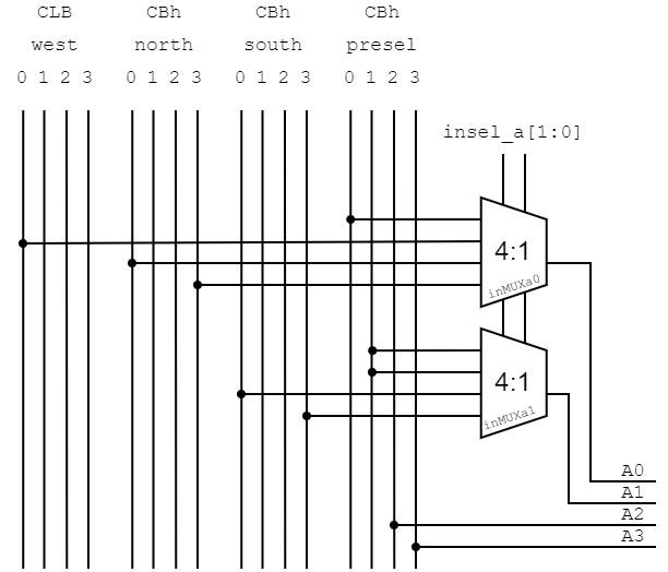 Fig 2: Input post selection multiplexer for a single LUT instance.
And seing the CLB in the broader 2D picture where it is interconnected with other logic elements, we have the concept in Fig. 3 where terms like “north” and “west” make more sense.
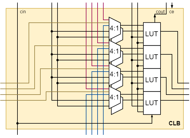 Fig 3: Concept view of the proposed CLB.
LUT Implementation
The next step is to build the LUT. Early on I knew that the LUT would be built using the good ol’ 74HC595 8 bit shift register.
It uses a straight forward SPI interface where the bitstream is shifted in and remains there for as long as the chip is powered on. There do not seem many alternatives which would offer 16 bits in a single chip so the 595 it is.
The LUT essentially consists of this memory and a big multiplexer selecting (looking up) the correct bit in the memory (table) for a given input.
Again 16:1 multiplexer do not seem to be such a common IC type. Therefore the smallest LUT in my design is going to be a LUT3 built with one 74HC595 and another 74HC151 as a 8:1 multiplexer. Two LUT3 can then be summarized to a single LUT4 with another 2:1 multiplexer which is easy to find.
Here several design options / questions arise:
- How big should the LUT be per bit?
- Is there a configurable option to split a LUT into a smaller LUT with more outputs? (e.g. a 6:1 LUT becomes a 5:2 LUT in Xilinx)
The first one is not easily answered. The more inputs a LUT has, the more complex logical functions can be implemented in a single LUT but resources are wasted if the logical functions are less complex. The fewer inputs a LUT has, the less LUTs are wasted on simple functions but multiple LUTs must be cascaded for more complex functions. The industry sweet spot seems to be around 6 bit input LUTs as they are currently used in Xilinx FPGAs. Mandatory reference to the infamous humor post about 8 LUTs. The second question regarding having two output bits per LUT I casually decided against because I simply have no easy way to deal with the extra output bits. Because it inevitably means that the output width of my CLB is doubled from 4 to 8 bits which do not natively fit on my 4+2 bit wide interconnect. And I simply do not want to expand the interconnect further as it already consumes lots of resources. There would have been one scenario where it would be useful to have at least an internal second output: the carry chain.
Full Adder with Look Ahead Carry Chain
I will preface this with a disclaimer: I implemented this feature for pure joy in implementing it, not because I expect it to perform better.
As far as I can remember, special carry chain hardware was introduced in FPGA hardware to make sum operations more performant. The performance bottleneck used to be propagating the carry bit of each bit in an input vector through another LUT instance.
This delay grew with longer input bit widths. Todays 16/18/25 bit quantized numbers would result in a cascade of 16/18/25 LUTs and subsequently a huge logic and routing delay with the MSB being the critical path.
The look ahead carry chain essentially pre-calculates the carry bit on every bit of the input vector and then quickly calculates the real sum with the help of an XOR gate and two multiplexers per bit.
I decided against this approach because it complicates the already complex input multiplexers and would add a little bit of (if we are being honest: neglectable) headache to implement the XOR and multiplexer in the bitstream.
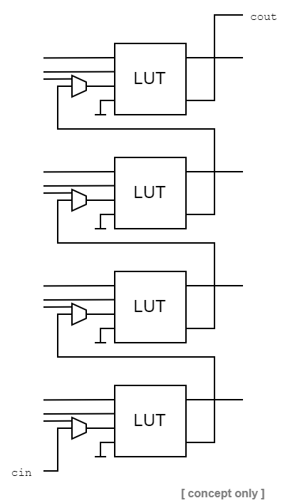 Fig 4: Concept of implementing the look ahead carry chain inside the LUT3 instance with an additional external multiplexer.
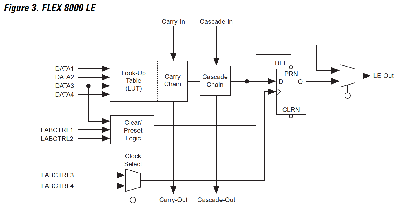 Fig 5: LUT with internal carry chain in the Altera FLEX 8000 FPGA architecture (Altera Flex 8000 Data Sheet)
Instead I implemented the carry chain like in the following diagrams.
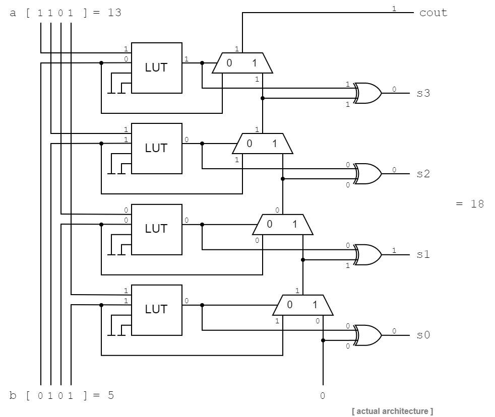 Fig 6: 4 + 4 bit full adder with carry chain showing an example where the unsigned numbers 5 (
0101) and 13 (1101) are being added.
Final LUT
Finally, we end up with a full 4 input, single output LUT in Fig. 7 or if you want the actual 7400-series implementation check out Fig. 8.
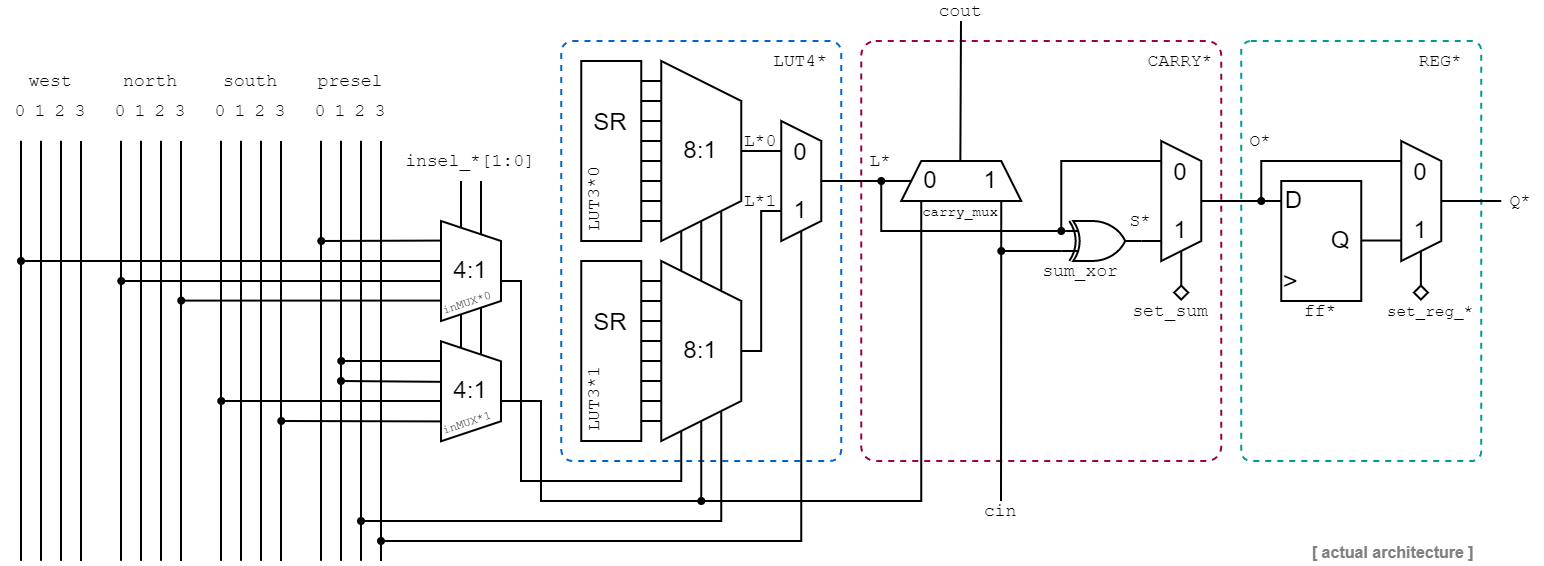 Fig 7: Complete and detailed diagram of a single
 LUT4 instance inside a CLB slice including the carry chain and the optional register stage.
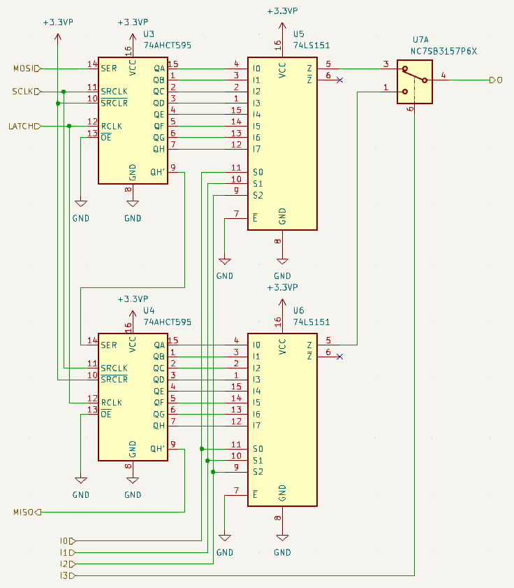 Fig 8: Single LUT4 instance schematics in kicad using
 74HC595 shift-registers as table and 74HC151 8:1 multiplexer as the “look-up” part.
(Note that I already fixed a bug in this Fig. 8 where I connected the ~OE pin to Vcc instead of GND)