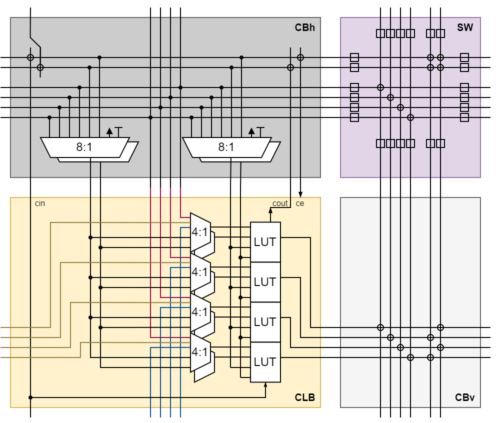
 Fig 1: One modular architecture tile consisting of a CLB, a SW box and two C-Boxes.
One slow morning at work with a touch too much of caffeine in my bloodstream I came up with the idea to build what is essentially the worst FPGA in history - on breadboards. Kinda how Ben Eater built his infamous 8-bit breadboard CPU. At first I put it off as yet another brain fart of mine because an FPGA would have to be vastly more complex to deliver a comparable computational power. However, the appeal of designing my own FPGA architecture did not leave my two brain cells alone that easily.
With a basic understanding how an FPGA is built, you can quickly make a few rough estimates of how big such a potential breadboard FPGA would be:
- to build a 4-bit counter, you need at least 4 LUTs with 4 inputs each
- the size of a 4-bit LUT amounts to 16 bits of “memory” in its configuration bitstream
- you would then use something like a 16:1 multiplexer to look up the correct value
- there is the 74HC595 shift register holding a whopping 8 bits of bitstream content
- therefore, a single slice holding 4 pieces of LUT4 instances would require at least 8 shift register ICs
- I want to build more than just a 4-bit counter and need more slices
Quickly, I realized that this would become a gigantic breadboard layout. And having built a rather less than more successfully working instance of the aforementioned 8 bit CPU, I knew I did not want to go down the solderless road with this project. It should be a modular PCB design. Once I had some understanding of the minimal requirements for the LUT part, I moved on to the bigger problem. You need a solid interconnect to connect all the LUT instances in a way that is both maximally flexible to connect things and minimally simple to configure via bitstream. This task turns out to be the real brain puzzle here.
Those of us engineers who work with FPGAs all know the trouble of how do you adequately explain what an FPGA is. Especially to people who are not completely outside of engineering. I am talking about fellow engineers who work in a different discipline like mechanical engineering or computer science. Usually, I start with the old breadboard approach:
What is an FPGA? “Immagine, you have a big array of memory chips all socketed on this big breadboard. Inside each memory you can define any digital logic function in the form of a look up table. Say, a counter. If you apply a number at the memory address input, the memory data output should result that number+1. But you could also implement arithmetic functions or state machines. All you have to do is connect the memories with jumper cables. That is what an FPGA is. A digital logic board where you can freely interconnect logic functions.”
The reality is a bit more nuanced. There are no jumper wires with near infinite connection possibilities but predetermined routing structures that can be connected using switches, giving a complex and finite way to connect logic cells. For the PCB FPGA I am about to build I can use bidirectional analog or digital MOSFET signal switches. You can easily find several of them on digikey. The problem is the scale. If you take the most flexible crosspoint matrix available, you will see that one single crosspoint is rather complex and consists of 6 individual MOSFET switches.
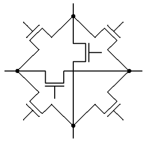 Fig 2: 6 MOSFET switches required to build a crosspoint with maximum flexibility. (S. Dutt et al. “A Search-Based Bump-and-Refit Approach to Incremental Routing for ECO Applications in FPGAs”)
If I were to apply this type of approach for my own architecture, I can estimate:
- 6 switch ICs per cross point
- a 4 bit FPGA should have at least a 4x4 crosspoint switch per logic slice
- 4x4x6 = 96 (!)
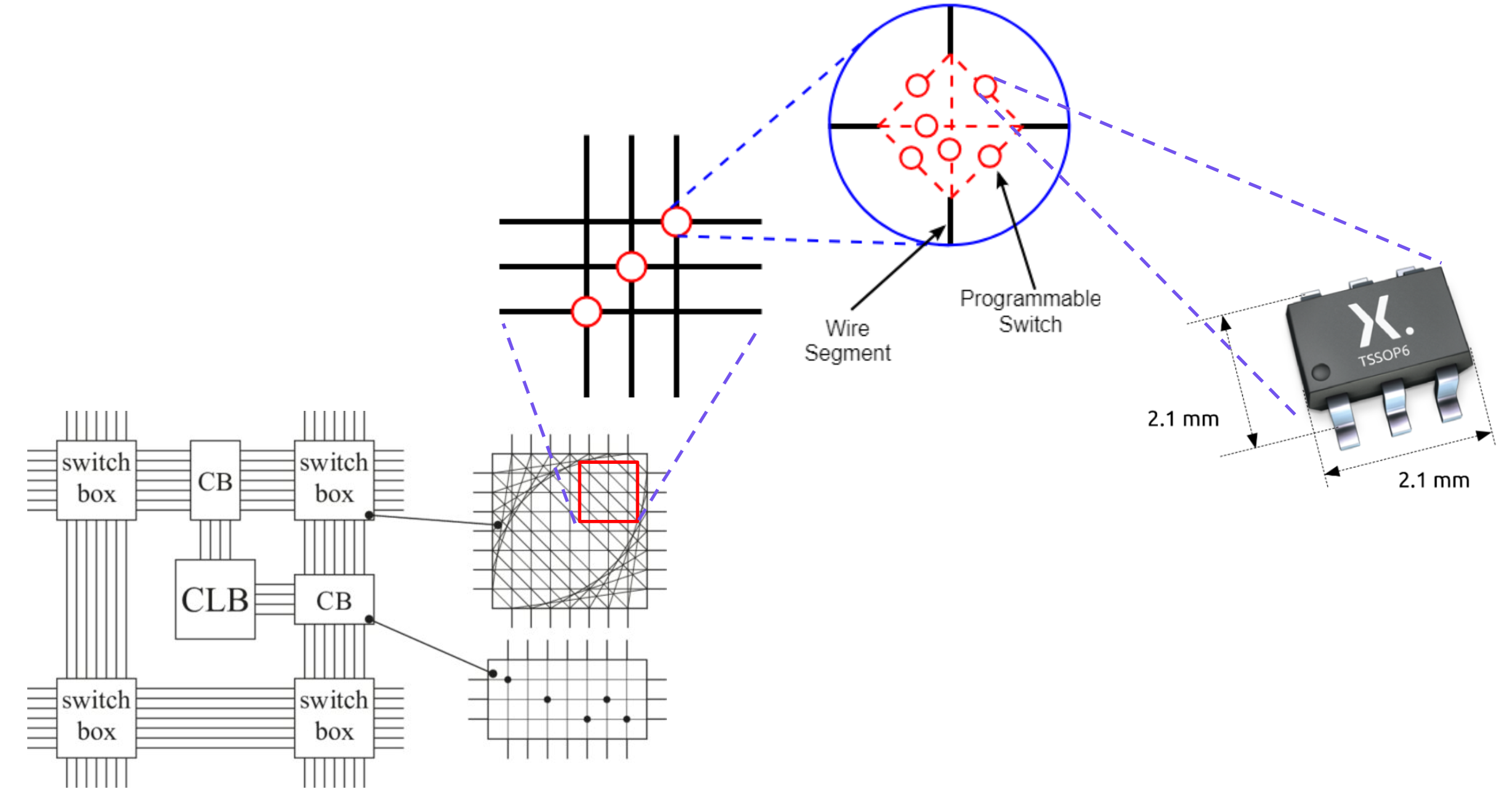 Fig 3: 6 switches per interconnect cross point using TSSOP6 MOSFETs for each switch)
That is an insane amount of SMT chips. This will be a multitude of pain in several design steps down the line:
- finding a switch IC which is cheap and has a digikey / JLC stock pile of ~1’000 pcs
- tight PCB layout of so many switches on a tiny ~5x5cm board
- soldering hundreds of SOT-23 ICs (or having them assembled error free)
- managing hundreds of bits in the bitstream and subsequential “compiler”
At this point I put the project on hold and decided it would be close to impossible (looooots of work and money) to actually follow through with the idea. However, during a Sunday brunch with my fellow engineering friend (and to the annoyance of his non-engineering wife) I would bring up the idea. As weeks went by, more and more ideas came into the whole architecture aspect of the design.
Remember, we are still talking about the shittiest FPGA ever created, but I did find reasonable compromises that would lead to a modular, FPGA-like 2D matrix architecture with the following characteristics:
- fully 4-bit capable (4-bit counter, arithmetic)
- fully modular and extensible, build it as big as you can pay for PCB modules
- less flexible but much simpler and resource friendly interconnect
- expandable with BRAM, I/O, PLL and other specialized tiles
Before I go on, I have to answer the question of: WHY?
This project is mostly only educational in nature. I had to research many lowest of low level features of modern FPGA architecture.
A knowledge that contributes to the everyday knowledge required for FPGA designs.
Also: As a (nowadays mostly) digital design engineer I miss my 3D CAD mouse (now supported in KiCAD) and snorting some exquisitely delicious solder fumes.
A rich history of FPGA architecuture
…of which i am going to ignore some parts because this project is definitely about reinventing the wheel and not about delivering state of the art performance.
FPGAs were invented some decades ago. Naturally, there has been a lot of research into efficient hardware as well as feedback from the industry regarding what architecture and features will be most efficient in practical applications. Most notably, the size of LUT inputs (more on that later) and the introduction of dedicated processing elements (DSP slices and Block RAM).
When I approached this project, I researched many old FPGA architectures (as they tend to be simpler) as well as newer ones. Keep this in mind when you continue reading about the atrocities I managed to frankenstein together. They may not be the simplest circuit to achieve the task or give any notable performance boosts - heck I am not even sure if my PCB sized logic cemetery is capable of running into the same timing problems as modern FPGAs. I lowkey hope that it is capable of having setup and hold time issues as it would provide a unique opportunity to poke around with a scope to show actual measurements of failed timing.
What my FPGA architecture does achieve though, is its availability as a passion project for me to dive deep into FPGA architecture, contemplate any possible applications that I may want to run on the hardware, figure out potential bottlenecks and mitigate them with my own solutions. My current end-goal (if I am ever to go there) is to expand the FPGA to a poster sized art piece having BRAM and analog peripheral I/O blocks to imitate a (awfully slow) version of an RF-SOC with a DDS demo running on it.
Architecture Concept
I went through several iterations of the overarching architecture that includes logic elements and interconnect. What I am about to present is the result I ultimately felt comfortable with going into production. I followed the approach where the FPGA fabric is divided into three (resp. four) major components:
- the Configurable Logic Slice (CLB) containing the LUTs
- the Switch Box (S-Box) for bus routing
- the connection box (CB) to connect inputs and outputs of CLBs to interconnect routes
The CB I went with has a horizontal (inputs) and a vertical (outputs) instance per CLB. This separation is something that is used in some FPGAs.
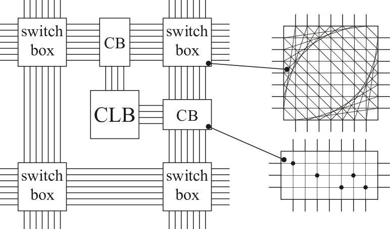 Fig 4: Simple interconnect concept with several S-boxes routing the interconnect and C-boxes connecting the inputs and outputs to the CLB. (P. Kaufmann, “Adapting Hardware Systems by Means of Multi-Objective Evolution”)
The architecture I dreamt up looks like the one in Fig. 1 above and in a broader sense with modular tiles like this:
 Fig 5: Multiple tiles can be stacked in 2D to build a full FPGA. More features like I/O and PLL resources can be added at the edge of this matrix.
In later posts on this blog I will dive further into the details of each block and why things are the way they are.
What I did evaluate on this architecture level though are, if it is efficient or possible at all to run certain applications on it.
Let me mention some of the features my proposed architecture has to show.
I decided for a 6 bit wide interconnect bus which I intend to use for 4 bit wide signals plus 2 more bits for “priority” signals like carry chain propagation. Having 2 more bits is generally good to relieve potential congestion or if you want to rout a control/enable signal to multiple parts of the FPGA.
The LUT outputs can be individually switched through to the vertical signal routing column with the vertical connection box (CBv).
The heart of the interconnect is the switch box (SW) which can route signals from any to any direction. Note that it has two types of switches: the enable switches which act as a bus separator and the crosspoint switches to make 90 degree distribution of signals possible.
Next is the horizontal connection box (CBh) which has a 4 bit output to its south pole into the CLB inputs.
A great help here was a comment online that input selection can be done using multiplexers instead of signal switches, facilitating a much simpler configuration. I went with 8:1 multiplexers to offer a great variation of input combinations for the CLB.
An important feature of the CLB is 4+4 bit addition. This has to be done by sourcing both the north and south bus directly as 4 bit input vector.
Another feature of the CLB and the interconnect is the direct east/west connection which allows LUT cascading without the need of interconnect resources (Fig 6). A task that in Xilinx FPGAs would be done using the MUXF7, MUXF8 etc. to combine multiple LUTs to a single output.
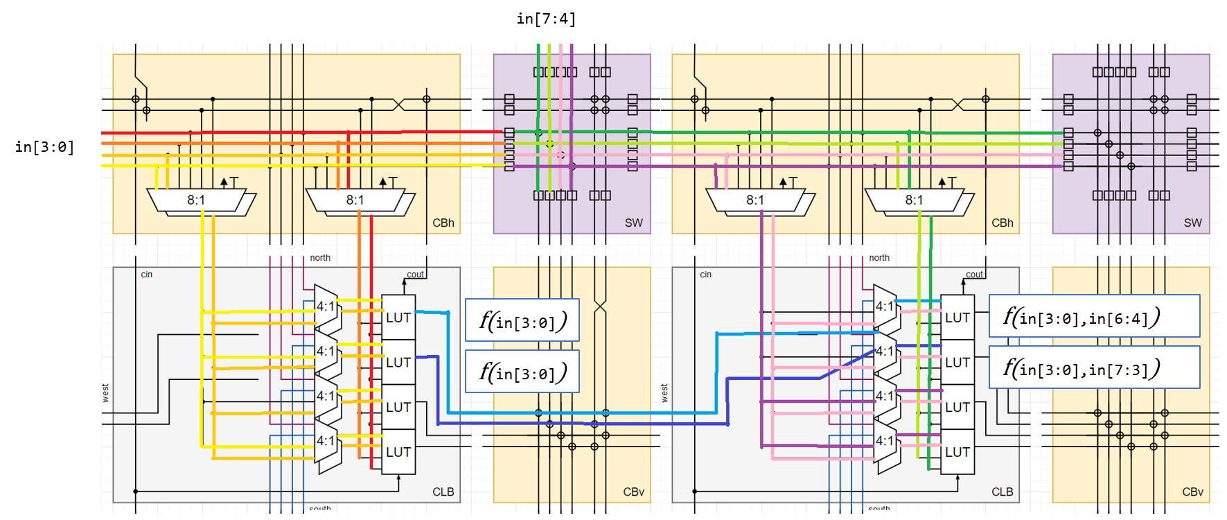 Fig 6: Cascading LUTs to expand function input arguments beyond 4 bit.
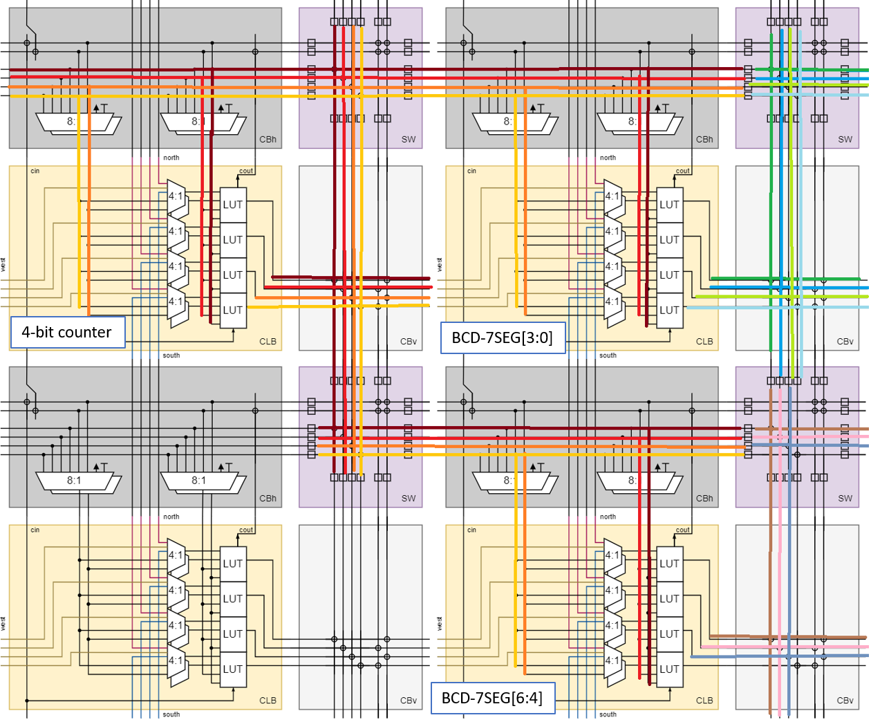 Fig 7: 4 bit counter with BCD to 7-segment decoder.
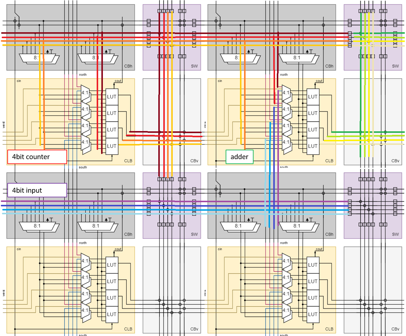 Fig 8: 4 bit counter with 4 bit adder to add offset value.
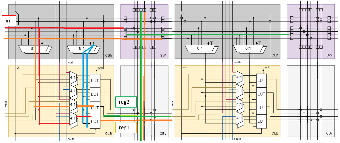 Fig 9: Looping back a single bit signal to create a double-flopped signal.
Honorable mentions
I am not the first person to have an insane idea like this. There is at least the Build your own FPGA project created for the Open 7400 Logic Competition