I love it when a plan comes together. This blog post is about three topics:
- expand the FPGA by another slice, forming a 1x2 FPGA matrix
- programing a rudimentary assembly “compiler” so I do not have to code bits by hand
- runing a 4-bit counter AND a fizz-buzz detector
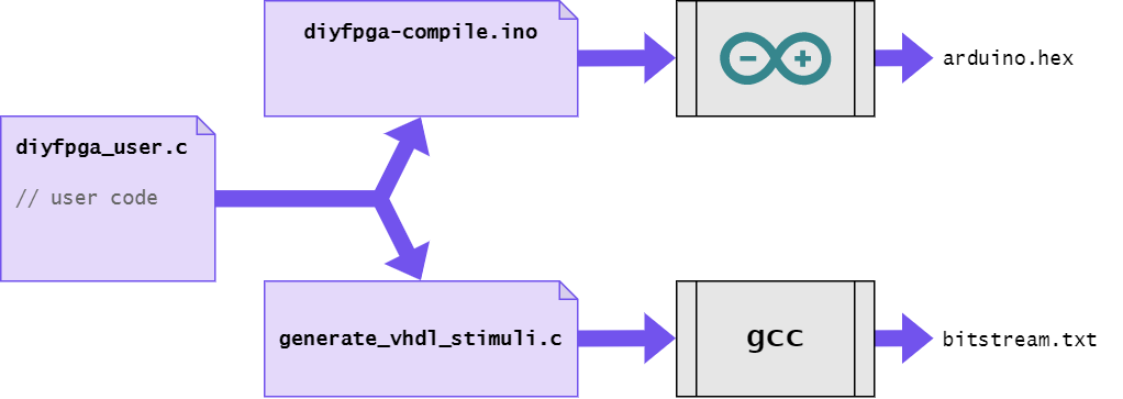 Fig 1: Single source - multiple targets.
The Compiler
The disapointment first: No, I did not build a complete place and route algorithm that maps any VHDL/Verilog code to my architecture. And I do not intend to do that either. Now to the update. My approach has always been to simplify the configuration of the bitstream into a slightly more intuitive way than looking up numbers of bit positions in a table. I do not want to count bits with the method explained in the previous post. What I want is an abstraction layer for the bitstream with mnemonics to enable certain features - sort of like an assembly language.
I will spare you the nightmarish details of ideas that I previously envisioned for this. Ultimately, I opted for a C-library, using struct objects that are interpreted as bit fields in the background. The same C code can be compiled either with Arduino (to upload to the FPGA) or locally with gcc to export a bitstream.txt for VHDL simulations. (I do not yet have a testbench for an FPGA larger than 1x1 slices)
How the compiler works
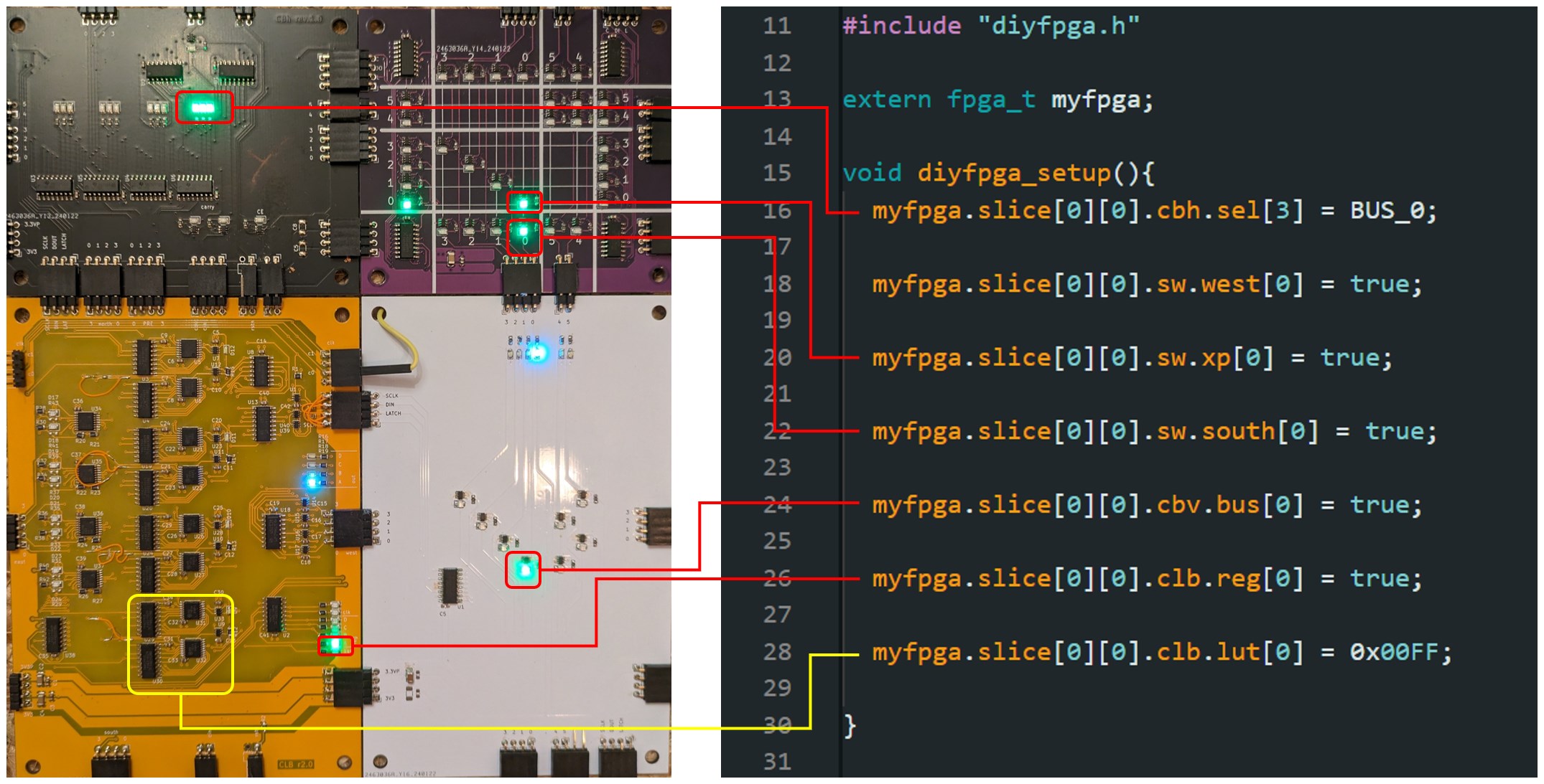 Fig 2: How different lines of code map to features on a single FPGA tile.
Consider the relationship between the lines of code in Fig. 2 to the enabled bits in the bitstream. At this point it should be evident why I picked green LEDs to highlight the bitstream configuration. It reminds me of the green wires in the Implementation view in Vivado. The gist of this way of coding is, that every bit in the bitstream now has a descriptive (although not very short) mnemonic to it.
Also note that I still use the Excel sheet to give me an instantiation vector for the LUT.
In this example I looped back the bus[0] signal and let the LUT invert it to achieve the good ol’ blinky. Note that my signal LEDs have the color blue.
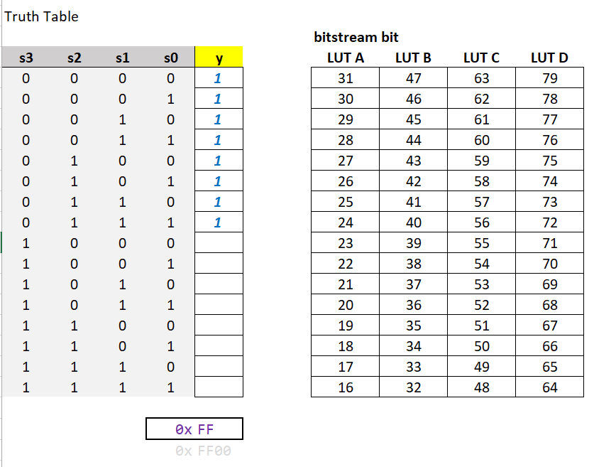 Fig 3:
 0x00FF is the LUT contents for an inverter bit acting on S3.
Reminder that modern FPGAs do support direct LUT instantiation with a hex vector: Xilinx UG953.
Blinky
With this approach the C-code can grow quite a bit longer for the necessary configuration of a bitstream for the previously described 4-bit counter.
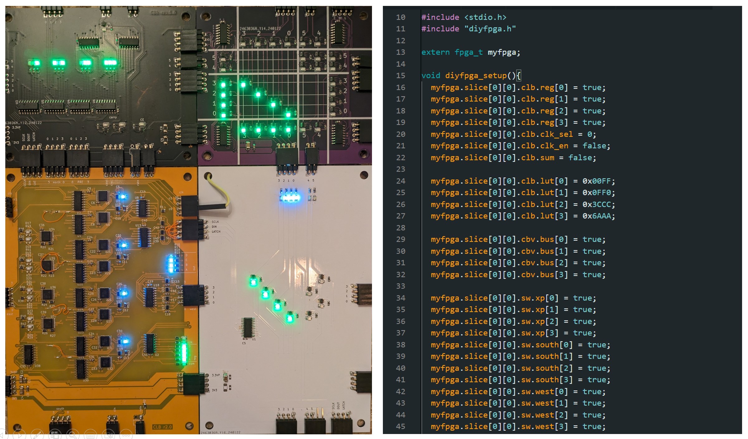 Fig 4: 4-bit counter first written in C to generate the bitstream.
Fizz-Buzz on multiple Tiles
By now I have a few assembled PCBs laying around. It is time to stack them together to thest a 2D matrix of tiles. At this point, a warning is necessary:
Warning: Using multiple FPGA tiles in a matrix configuration inherently provides you with multiple OUTPUTs from CLBs. The compilation process using C cannot detect issues where multiple drivers are connected through the selected routing options. This creates the potential to connect two outputs together which can damage the hardware.
Caution and/or bitstream simulation in VHDL is advised.
Fizz Buff is a well known tech interview question. On a sidenote: I am curious if you could build a high performance fizz buzz on FPGA and send it over 100G ethernet to the CPU to beat the High throughput Fizz Buzz challenge. Anyways, in my case Fizz-Buzz is an easy extension to the 4-bit counter.
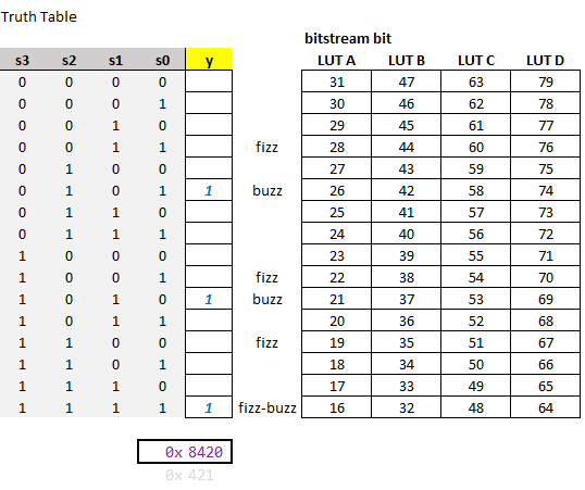 Fig 5: Creating the LUT contents from the truth table of Fizz-Buzz.
I connected the 4 signals of the counter that are in the loop for the counter to the inputs of the 2nd CLB. Next, only 2 LUTs of the CLB are used to output 1 on either the number 3 (Fizz) or 5 (Buzz). And just because I can, I routed the Fizz and Buzz signals back up north parallel to the existing 4-bit counter.
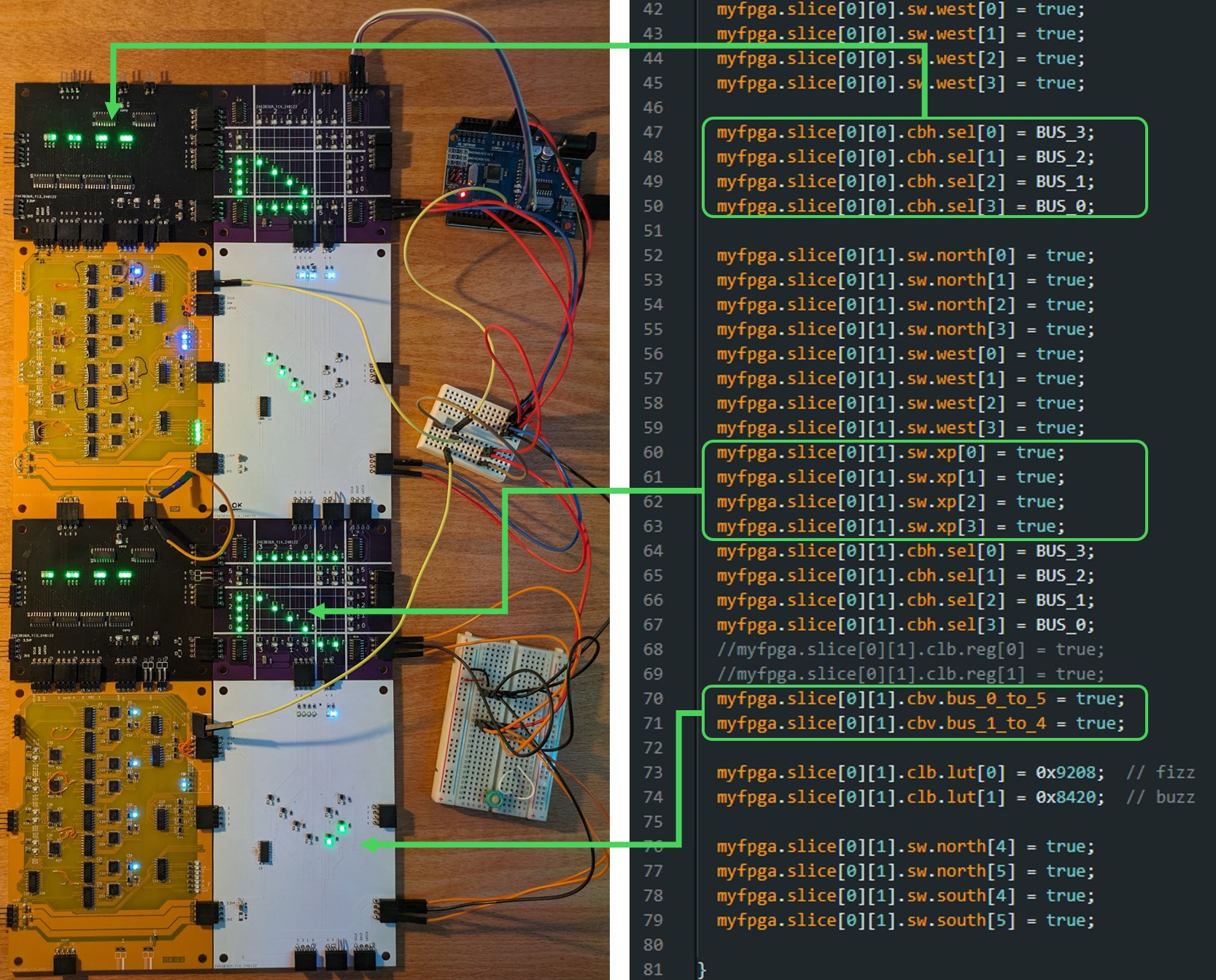 Fig 6: Programming the FPGA using the Arduino library.