Since the completion of the most complicated modular PCB module, the CLB, I have successfully assembled the surrounding interconnect PCBs. As it turns out, you can reflow solder PCBs on the stove in your kitchen. In unrelated news, does anybody have tips on how to get rid of unwanted smells in your apartment?
Moving on… In theory, my PCB design should match the previously designed VHDL model. In practice, I messed up the byte order on the switchbox PCB (which was a pain to layout precisely because of the byte order). Other than that, all of the SW, CBh and CBv are working flawlessly - just as designed. It is now time to verify the hardware against the previously built bitstreams for the VHDL simulation. But how do you program an FPGA by bitstream directly?
What I am about to do is to manually layout a design into an existing FPGA architecture. Similarly to programming a CPU in assembly. This workflow is highly unusual or even unavailable for modern FPGAs. In FPGA designs, the designer describes the behaviour of a circuit. Only then the tool will map this to hardware in two steps: place & route.
The Blinky Example
1. Place
Currently, my FPGA consists of only a single tile containing one CLB slice with 4 LUTs available.
There is not much to place. For a single blinky-bit, only one of the four LUTs is required. I will pick LUT A (or LUT 0).
One LUT4 instance contains a 16-bit long truth table that must be programmed.
And by the way, this can be done on modern FPGAs too by manually instantiating a LUT primitive and define its contents as a hex vector: Xilinx UG953.
Since counting to 16 with your fingers is quite tedious I created a table to map the bits to a given truth table.
This is more of a visual aid rather than a complex tool.
See Fig. 1 where the toggle bit at the output Y is inverting the input S0. To map this truth table to LUT A one has to map the 1-bits from the Y column to the bitstream address of the LUT A column. In other words, if there is a 1 in the Y column the corresponding bit in the bitstream must also be 1.
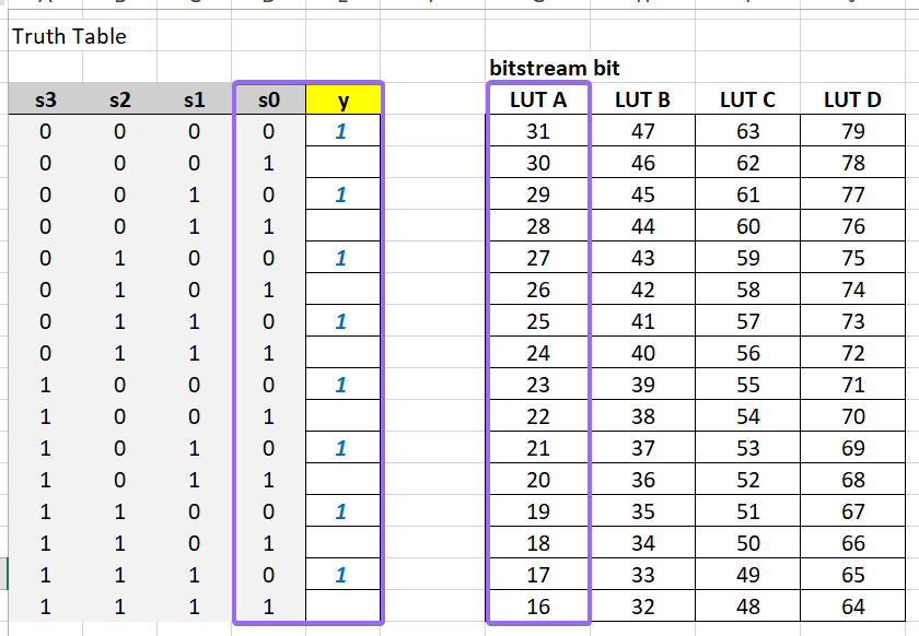 Fig 1: Truth table for a (
lut_truth_table.xlsx).
Finally, the CLB (containing the LUTs) has a few features that need to be enabled.
For proper RTL (register transfer logic) operation, the register must be enabled via en_reg_lut_a at bit (15).
2. Route
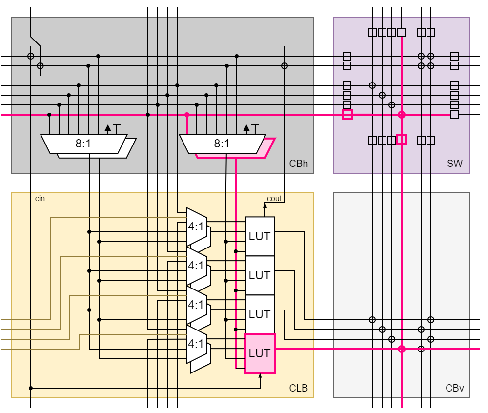 Fig 2: Schematic of the loopback routing of a single bit.
The LUT A is set up to invert the input signal. What is left is to route the output back to the input as shown in Fig. 1.
The LUT output bit will exit the CLB on the 4-bit wide bus at position [0] and enter the vertical connection box (CBv) on its west input bus.
To connect this signal to the horizontal routing lines the crosspoint xp_bus[0] must be enabled.
This is done by setting a 1 at the corresponding location in the bitstream. In the case of xp_bus[0] this is bit 7 as indicated by the bitstream documentation in Fig. 3.
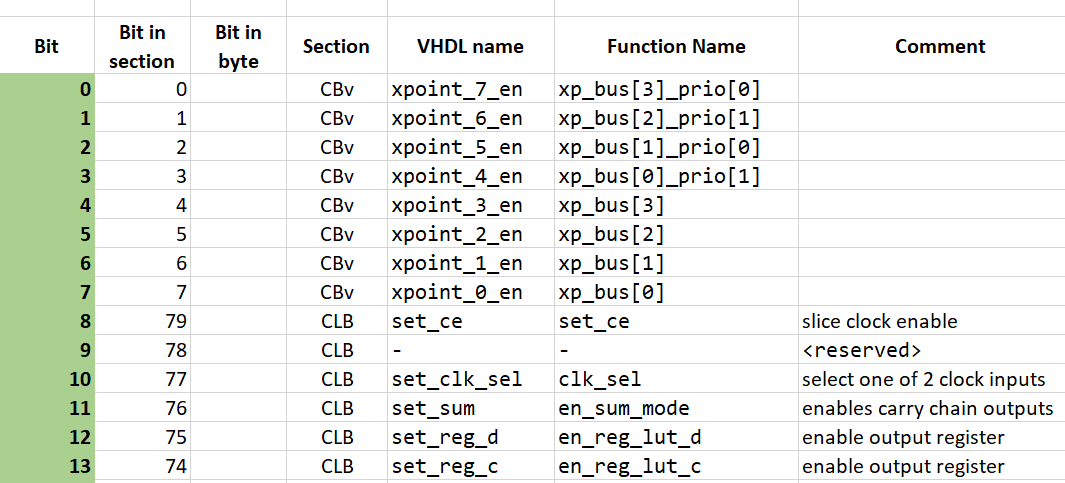 Fig 3: Excerpt from the bitstream documentation containing the CBv settings (
bitstream_doc.xlsx).
The signal will now arrive at the south bus of the switch box (SW). Before the signal is allowed onto the switch matrix it has to pass the gate at the edge.
This has to happen once for the incomming (en_bus_south[0]) and once for the outgoing (en_bus_west[0]) signal. And finally, the crosspoint switch (xp_bus[0]) on the switch matrix itself has to be activated.
In total three bits must be set per signal.
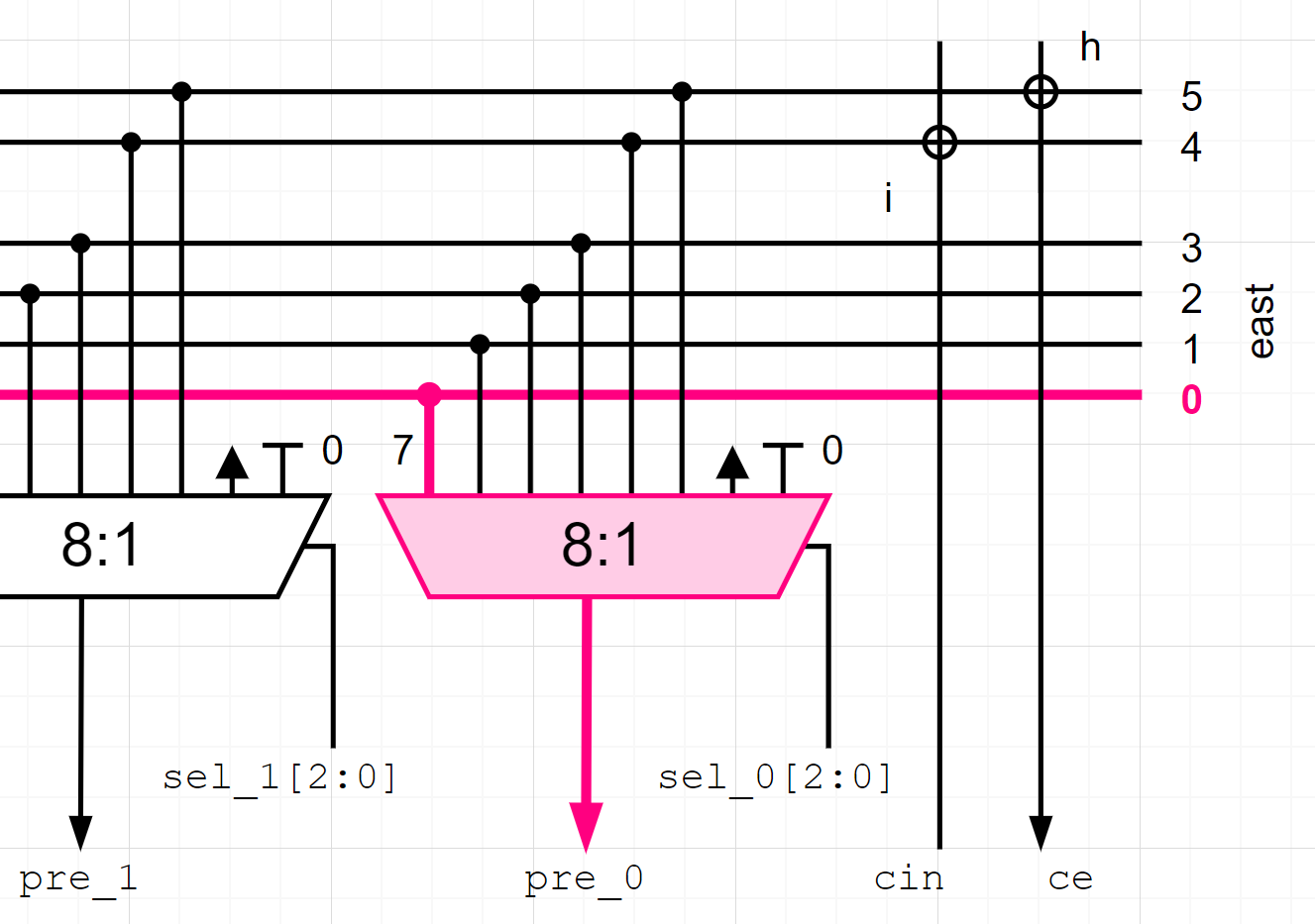 Fig 4: Input multiplexer to the LUT.
Next, the horizontal connection box CBh creates the input selection for all the LUTs in the CLB. The unprogrammed value will default to GND.
Therefore, a corresponding value must be programmed to select the correct input signal from bus[0].
This is done with three bits named presel_0[2:0] which will serve as an address to the 8-input multiplexer.
To select the bus[0] line, the multiplexer must be set to input 7 (as shown in Fig. 4) which translates to presel_0[2:0] = "111".
Code
Before uploading the bitstream to the actual hardware, it can be simulated with the previously built VHDL model.
A pyhton script can build the bitstream for the testbench from the bit addresses that need to be set to 1 as described above.
conf_bits = []
conf_bits.append(7)   # CBv LUT A -> bus[0] enable
conf_bits.append(111) # SW xpoint_1 south[0] to west [0]
conf_bits.append(119) # SW en_bus_south[0]
conf_bits.append(127) # SW en_bus_west[0]
conf_bits.append(101) # CBh presel_3[2] = +4
conf_bits.append(102) # CBh presel_3[1] = +2
conf_bits.append(103) # CBh presel_3[0] = +1
conf_bits.append(15)  # CLB LUT en reg a

for b in [17,19,21,23,25,27,29,31] :
    conf_bits.append(b)
For the upload to the hardware, I still use an Arduino and the corresponding C-code looks similar:
#define BITS_CONFIGURED 15

char conf_bits[BITS_CONFIGURED] = {
   7,   // CBv: enable LUT_a output
   111, // SW:  xp_bus[0]
   119, // SW:  en_bus_south[0]
   127, // SW:  en_bus_west[0]
   101, // CBh: presel_0[2] --> MUX addr +4
   102, // CBh: presel_0[1] --> MUX addr +2
   103, // CBh: presel_0[0] --> MUX addr +1
   15,  // CLB LUT en reg a
   17,19,21,23,25,27,29,31}; /* LUT A */
So there you have it: assembly language for FPGA
Simulation
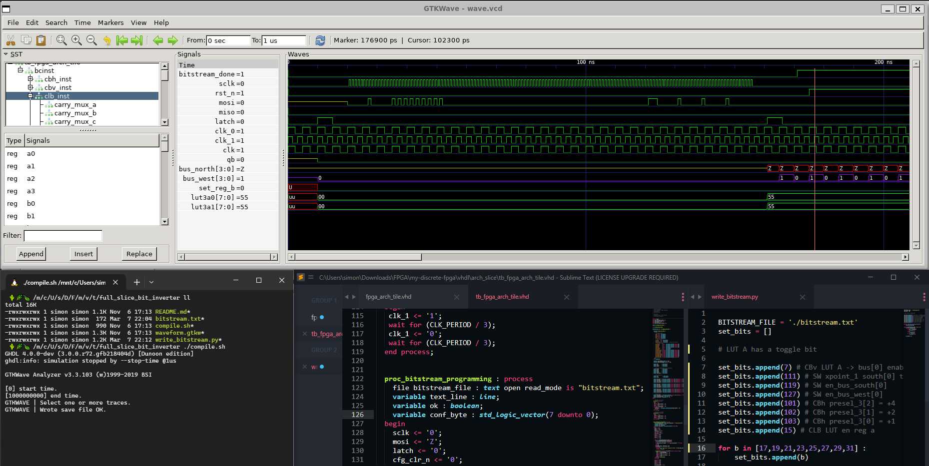 Fig 5: The VHDL simulation workspace programs the bitstream into one FPGA tile and simulates its behaviour: a toggling bit.
Run on actual hardware
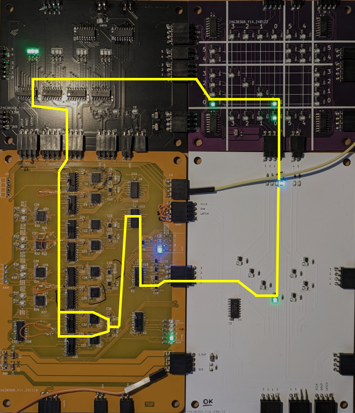 Fig 6: Visual aid of how the configuration is routed on the FPGA tile for a single toggle bit.
F-max Estimation
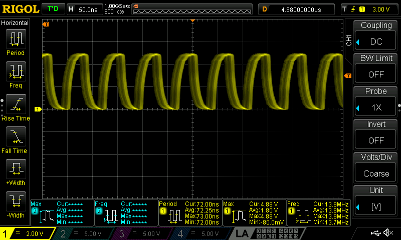 Fig 7: Scope view of the ring oscillator with a frequency of 13.9 MHz.
With the hardware working, I can now test the maximum speed of my FPGA by building a ring-oscillator.
To do so, I just disable the output register (en_reg_lut_a / bit 15) to switch from RTL to combinatorial logic.
My osciloscope tells me a toggle rate of some 13.9 MHz (!). This makes me happy.
Because in my wildest dreams, I am already considering adding some DSP capabilities with shared hardware.
Let’s say, you have an audio signal, sampled at 8-bit / 44.1 kHz while the larger FPGA runs at a conservative 5 MHz.
Then you would have approximately 100 clock cycles per sample to perform some DSP. That may be enough for quite a few FIR taps.
I hope 5 MHz is achievable since this ring oscillator is the shortest possible timing path on my architecture - it will only grow from here.
Conclusion
All-in-all a great first success. I would say, the greatest challenge so far is not the hardware itself - 7400 logic is simple and straight forward. No, the challenge is keeping both the VHDL model up-to date with the PCB (or vice versa). For example with rev. 2 of the PCB for the CLB I decided last minute, I need a clock enable for the flip flop. Luckily, I had some unused “reserved” configuration bits left both on the CLB and the CBh. Changing such a thing required me to go back to the VHDL to implement and test this feature there as well. But then of course, a lot of testing is required to ensure that a given bitstream produces the same results in the simulation and on the hardware.