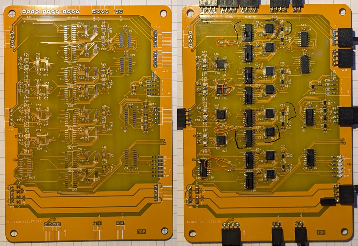
 Fig 1: PCB before and after assembly and debugging.
A month or so after sausageing around in KiCad I have some fresh PCBs on my desk ready for prototyping. (Not for the life of me! did I want to make this a 4-layer PCB even though we live in 2024 and there are virtually no good arguments against 4-layers anymore. anyways.) The boards look pretty. And yellow. Just like in the drawings I made.
In theory, theory and practice are the same. In practice, they are not.
Well, in theory my digital twin (in VHDL, see previous article) and whatever I assembled on the PCB are the same.
The first fuckup that was noticeable was the wrong polarity on the output enable (~OE) of the shift registers.
This condition made itself noticable by being a classic implementation of a WOM (write only memory).
I had to embark on a mission to attach a modwire on every single shift register ~OE pin after which all lights started flashing and blinking like a disco.
So I went ahead and implemented the 1-bit counter (inverter) on the PCB. It worked!
The next logical thing to test is a 2-bit counter which I immediately uploaded and saw it blink the wrong way.
I went back to the VHDL model but it did not spark joy to build another testbench just to figure out the wrong bit.
Now here is a different approach: Test your digital design with an Arduino as the testbench.
Because I figured,
- a) I am quicker with breadboard wires and with C-code on an Arduino (vs. generating incremental stimuli data in Python and write a new VHDL testbench)
- b) the error(s) are more likely due to bad soldering on the PCB anyways
What I came up with is shown in Fig. 2.
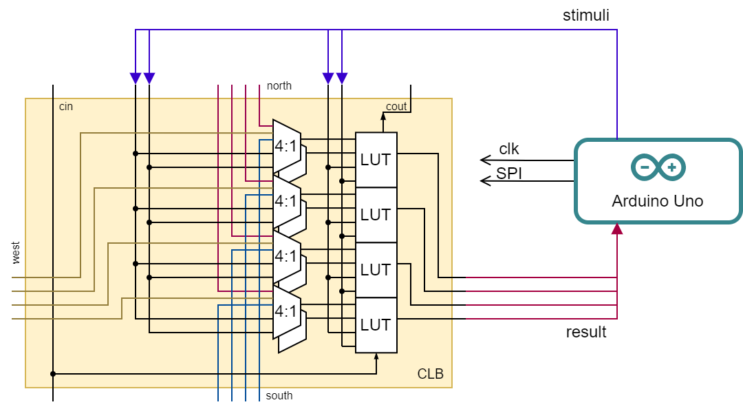 Fig 2: Testbench approach with an Arduino Uno to provide bitstream, clocking and stimuli data and read back any results.
Thechnically, I had documented the bitstream before in an excel sheet.
Because I absolutely needed this for when I want to set bits according to a truth table.
Let’s see how the second bit should behave when implemented in LUT.
Note that the counter input bits are in reversed order - bit 0 is marked m and bit 1 is marked s2.
Since we are now using LUT_B this table tells me that I need to set the bits 36 to 43.
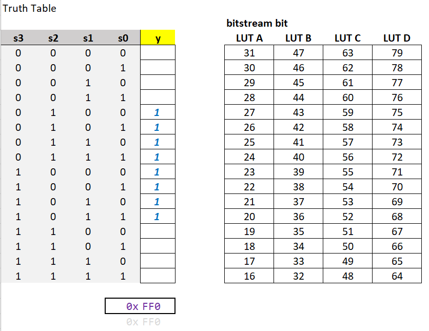 Fig 3: Truth table for bit[1] of a counter.
Well, here is where it blinked the wrong way. So I coded an Arduino script which does the following things:
for each LUT in LUTs:
   for each bit in conf_bit:
      program_bitstream(bit)
      for each stim in input_vector:
         write(stim)
         clock_pulse()
         read(result)
         if(result)
            print("1")
         else
            print(".")
This will print a matrix of how the LUT behave to all input stimuli given all single bit configurations. The output looked a bit like this:
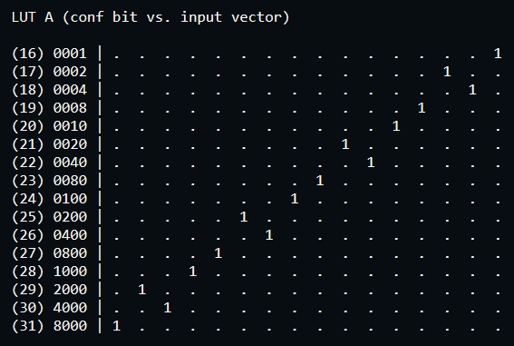 Fig 4: Measured LUT output behaviour for LUT_A.
Now each configuration bit should act upon exactly one single input vector to produce a 1 at the output. What we see here is some type of bit flip. And promptly, if I check back with the KiCad schematics, I produced a bug all by myself. The VHDL simulation would not have caught this.
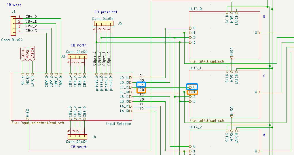 Fig 5: Concept view of the proposed CLB.
Another journey into modwire-land later, we have this problem sorted. However, there was more trouble.
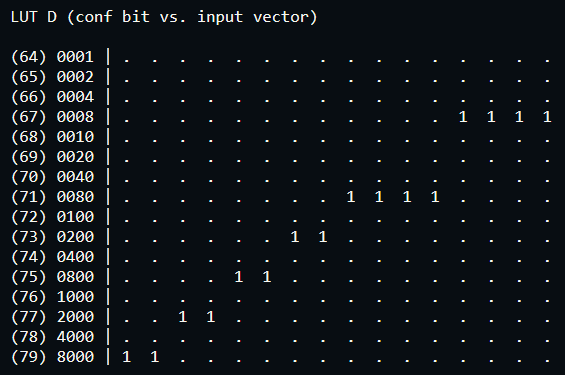 Fig 4: Measured LUT output behaviour for LUT_D.
I’ll spare you the details (because I don’t actually know them myself) but this problem was caused by several bad (cold) solder connections. After resoldering a bit of everything, it worked and produced a clean diagonal line of 1’s. Now I can use the above truth table in Excel to create the remaining LUT functions of an entire 4-bit counter. And it works!!
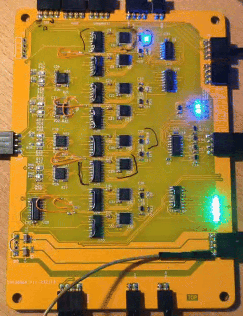 Fig 5: 4 bits counting ahead…
We end with a first conclusion: Yes, it is possible to waste dozzens of 7400-family ICs to recreate half of a single 7400-family IC. I am thrilled to expand this project further.