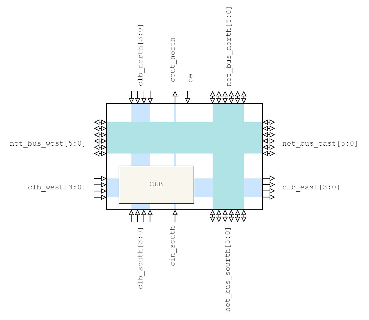
 Fig 1: Top level diagram of a modular
 slice.
Now we can build an entire architecture slice consisting of both the CLB and the associated connection boxes and a switch box.
I have decided that this is the smallest modular building block of my FPGA.
Therefore, the bitstream management becomes a lot easier if it is also handled modularly like this.
The bitstream enters the slice from the north into the SW box and continues to the west to the CBh, then down into the CLB and east to the CBh from where it is routed south again into another slice. See Fig. 2 for reference.
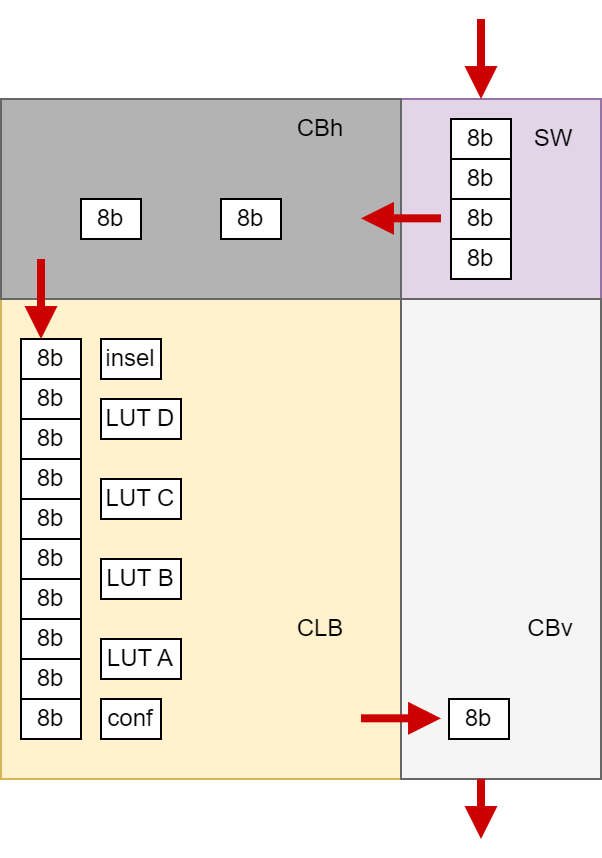 Fig 2: Bitstream flow through the
 slice.
I then documented this bitstream order in a table:
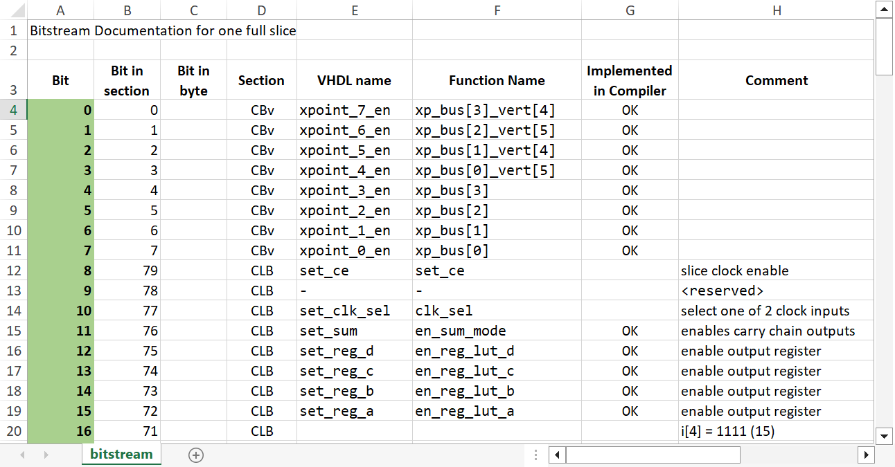 Fig 3: Top few rows of the bitstream documentation.
Using this documentation I can then reference all the bits that I need to set to configure a desired function.
For example. I want to implement a single bit that is looped back and used as the LUT input again to make it the opposite value (bit = !bit). A simple inverter. Which will output a toggle bit signal at half the clock frequency.
For no particular reason, I pick LUT_B and output Qb.
In the bitstream reference I can see that I have to enable the D-type flip flop by setting bit 14 to 1.
I then connect the output Qb to the CBv bus using bit 6.
This signal will arrive at the switch box where I have to make appropriate connections so that the signal ends up on the horizontal CBh where it can be selected as a LUT input.
I do this by enabling the input (126) and output bits (118) as well as the crosspoint switch (134).
Next, I configure the CBh to select the signal as LUT input. The signal is on the bus[1].
The input multiplexer therefore selects it on position 6 (or 110 in binary) therefore bits 89 and 90.
In python this looks like the following code.
Note that I also configure the actual LUT contents by setting the entire half of the LUT (bits 40 to 47) to 1.
This matches with my choice to use LUT input [3] which is implemented as the 2:1 multiplexer selecting the top or bottom half of the LUT4. More on configuring the LUT contents follows in the next article.
1
2
3
4
5
6
7
8
9
10
11
12
13
14
15
16
17
BITSTREAM_FILE = './bitstream.txt'
set_bits = []

# LUT B has a toggle bit

set_bits.append(6) # CBv LUT B -> bus[1] enable
set_bits.append(14) # CLB LUT en reg b

set_bits.append(89) # CBh presel_3 = 6
set_bits.append(90) # CBh presel_3 = 6

set_bits.append(134) # SW xpoint_1 south[1] to west [1]
set_bits.append(126) # SW en_bus_south[1]
set_bits.append(118) # SW en_bus_west[1]

for b in [40,41,42,43,44,45,46,47] :
    set_bits.append(b)
The python script outputs the bitstream as a file of 1’s and 0’s to be readable by the VHDL testbench.
All the testbench does is upload the bitstream to the slice and generate a clock signal.
So let’s run the simulation.
Sidenote: I use WSL 2.0 on Windows which can be tricked into running Linux GUI applications. I can therefore simulate my VHDL using GHDL and inspect the waveforms using the gtkwave GUI.
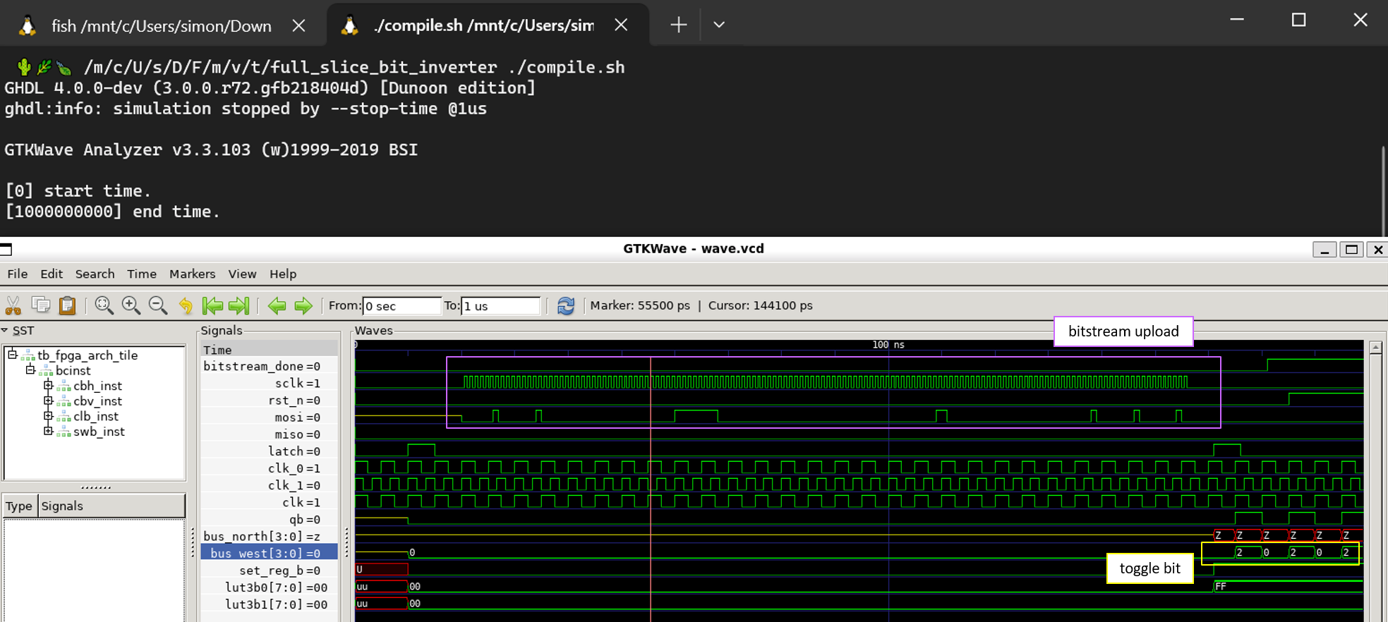 Fig 4: Compile and view waveform of the bitstream upload and toggle bit function on
 bus[1].
Great success! We have a toggling bit. And that is about all the testing I will do before proceeding with the circuit board layout. Let’s see how that goes.